
Part 2: How XYZ Pads Work
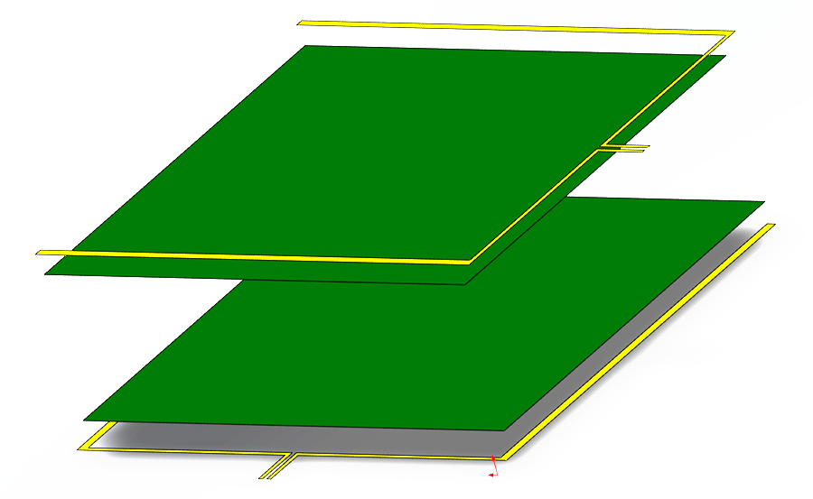
An XYZ Pad Sensor is comprised of two substrate layers, illustrated in the diagram below. Each layer is covered by a square or rectangle of resistive ink, which is connected to a conductive strip at both ends.
Typical construction diagram:
...And here's a 2-dimensional version, with labels.
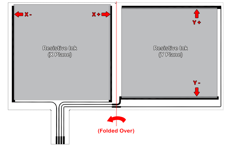
Elements on the two substrate layers are oriented perpendicular to each other, such that each layer forms a plane corresponding to an axis (X and Y). Here's how we'll read position and force, in a nutshell:
To read X position, apply a voltage across the X-plane, and read the voltage from either Y conductor.
To read Y position, apply a voltage across the Y-plane, and read the voltage from either X conductor.
To read force (Z-axis), apply a voltage a voltage from one X conductor to one Y conductor, then read voltages at the other X and Y conductors. The difference between these two measurements gives the voltage
drop between the two layers, and thus the relative contact resistance, which is proportional to force applied.
Functionally speaking, there's not much more that we need to know. But if you found the abridged explanation unsatisfying, recall that XYZ Pads operate very similarly to 4-wire resistive touch screens / pads. There are already some great appnotes (from Atmel, TI, etc.) that break down the details, so we'll skip re-inventing that wheel.
Up next, some breadboarding...